test CMOS INV (tran)

**** CMOS INV ****
mn1 t2 t1 0 0 nm l=4u w=8u ad=80p as=80p pd=36u ps=36u
mp1 t2 t1 t3 t3 pm l=4u w=16u ad=160p as=160p pd=52u ps=52u
c1 0 t1 3p

**** power suplly ****
vdd t3 0 dc 5
vin t1 0 pulse( 0 5 30n 2n 2n 100n 200n)  (←下図に描く形のパルス入力)

**** MOS FET model ****
.model nm nmos (level=2 vto=1.0 tox=0.035u nsub=1e15 uo=500
+ ucrit=4.5e4 uexp=0.11 tpg=1 ld=0.2u xj=0.29u js=6m pb=0.94
+ cj=3.85e-4 cjsw=1.6n cgdo=0.45n cgso=0.45n cgbo=0.042n
+ rd=1 rs=1)
.model pm pmos (level=2 vto=-1.0 tox=0.035u nsub=1e16 uo=250
+ ucrit=2.0e4 uexp=0.08 tpg=-1 ld=0.3u xj=0.43u js=6m pb=0.88
+ cj=1.23e-4 cjsw=2.36n cgdo=0.25n cgso=0.25n cgbo=0.02n
+ rd=1 rs=1)

.tran 5ns 200ns
(↑ここが重要! 5nsごとに200nsまでの過渡解析をさせる)
.print tran v(t1) v(t2)
(↑端子t1と端子t2にかかる電圧の過渡解析結果出力する)
.plot tran v(t1) v(t2)
(↑端子t1と端子t2にかかる電圧の過渡解析結果を簡単なグラフにする)
.end
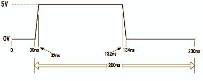
入力波形
|